EXF OPTICALNetwork components Project brief
Optical reference library

High-precision optical module testing equipment

High-precision optical module testing equipment
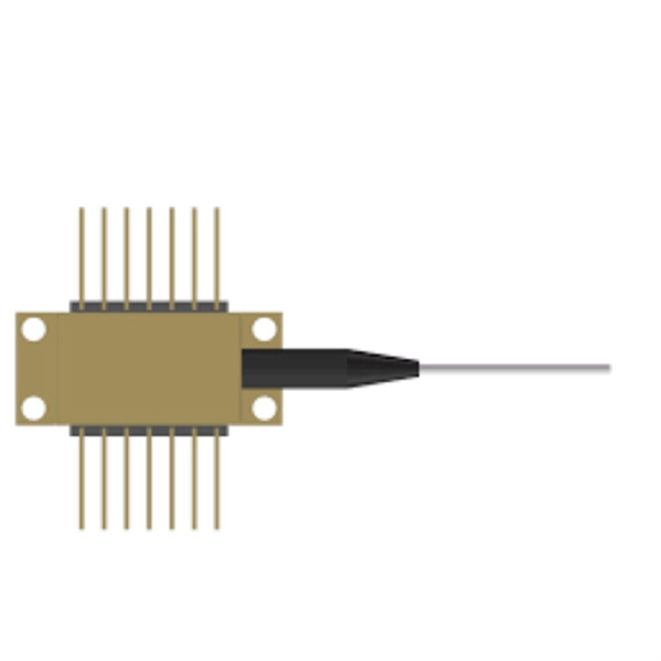
Illustrative equipment reference
Download PDF
Article contents

High-precision optical module testing equipment enables accurate characterization, validation, and quality control of optical components and photonic devices across R&D and production environments. Leading Equipment and PlatformsNEXUSTEST offers advanced test instruments for high-speed optical modules, laser diodes, silicon photonics wafers, and co-packaged optics devices, focusing on high-end optical and semiconductor testing solutions. Yokogawa's Multi Application Test System (MATS) provides a unified platform for high-precision, high-throughput testing of optical devices, transceivers, and photonic components.

It integrates optical and SMU modules, supports hot-swappable reconfiguration, and ensures stable, repeatable measurements for R&D, new product introduction, and volume manufacturing.

MAT

S is compatible with instruments like optical spectrum analyzers (OSAs), wavelength meters (WLMs), bit error rate testers (BERTs), and high-speed oscilloscopes, and supports LIV testing for silicon photonics devices. Keysight Technologies offers a broad portfolio of photonic and optical test solutions, including XP-class photonic component analyzers, coherent transmission testers, and modular test systems. These systems enable precise measurement of modulated optical signals, error vector magnitude (EVM), Q-factor, and phase error, supporting high-speed data center networks and complex optical component characterization.

Keysight also provides optical spectrum analyzers, tunable lasers, power meters, optical attenuators, and dispersion analysis tools for scalable test setups.

JP

T Laser Module Testers combine laser modules with high-precision automated optical inspection (AOI) systems. They are designed for evaluating optical component performance under monochromatic light of different wavelengths, suitable for optical device calibration, semiconductor manufacturing, 3D scanning, and scientific research experiments. Jenoptik develops high-precision optical systems and microoptics for semiconductor equipment, covering the full spectral range from deep ultraviolet (DUV) to far infrared (FIR).

Their solutions include objective lenses, beam shaping optics, gratings, and wavefront measurement systems, enabling precise inspection and testing of semiconductor structures and photonic devices.

Key Features to Consider

Measurement Accuracy and Repeatability: Essential for validating optical power, wavelength, and modulation characteristics.

High-

Speed Capability: Supports testing of high-speed optical modules and coherent transceivers. Modularity and Flexibility: Hot-swappable modules and platform-specific configurations allow adaptation to different device types. Integration with Production Lines: Systems designed for 24/7 operation in volume manufacturing environments.

Support for Multiple Wavelengths: Enables testing across the visible, near-infrared, and far-infrared spectrum.

Applications

Characterization of optical transceivers and photonic integrated circuits (PICs)Silicon photonics device testing, including LIV and modulation analysisSemiconductor inspection and calibration of optical componentsR&D and high-volume manufacturing of laser diodes, co-packaged optics, and optical modulesScientific research requiring precise optical measurements and beam shaping High-precision optical module testing equipment is critical for ensuring performance, reliability, and compliance with industry standards in photonics and semiconductor applications. Selecting the right platform depends on the required measurement parameters, throughput, and integration needs.

Photonic and Optical Test They support complex characterization and validation across a wide range of optical components and systems. Designed for precisio.

From reference to enquiry

Questions for your project

Use these editorial prompts alongside the linked excerpts. They identify items to confirm for your project.

Detailed reading

Distribution and installation references

Photonic and Optical Test

They support complex characterization and validation across a wide range of optical components and systems. Designed for precision, accuracy, and flexibility, these

Optical Component Test System

The Multi Application Test System (MATS) is an integrated platform for high-precision, high-throughput testing of optical devices, transceivers, and photonic components.

Worldwide standard for optical metrology

We offer optical measurement and manufacturing systems for quality control and assembly of lenses, lens systems, camera modules.

Optical Test Equipment | ISO Calibrated | Micro Precision

Every optical test instrument sold by Micro Precision is tested and verified operational before shipment. ISO/IEC 17025 accredited calibration is available for all instruments, providing NIST-traceable

Optical Test Equipment | Yokogawa Test&Measurement

Build integrated test systems with light source, switches, attenuators, SMUs, and OPMs to evaluate photonic subsystems.

DIMENSION

Offers precise, cost-efficient optoelectronic signal and anomaly testing for high-speed transceivers. For single-core fiber testing, various models available; supports FTTx diagnostics and network

Optical Test Equipment & Measurement Systems

Browse our collection of optical test equipment and measurement systems that uses precision optical technology to measure the properties of light.

1.6T/800G MPO Optical Module Testing Solution-

To ensure the performance and reliability of such modules, systematic testing solutions and high-precision instruments must be adopted. This paper proposes

Product Portfolio | TRIOPTICS

We provide the right solution for each of your individual needs. Discover the best of the TRIOPTICS product world here.

Optical Test, Measurement and Inspection Solutions

HOMMEL ETAMIC offers high-precision optical, tactile, and pneumatic measurement and inspection systems for analyzing the surfaces, shapes, and dimensions of your workpieces.

Kamera-Module Market in Saudi Arabia | Report

The production of high-precision camera modules requires capital-intensive cleanroom facilities, precision optics assembly equipment, and advanced semiconductor packaging

WORLD WIDE WEB JOURNAL Home

By clicking download, will open to start the export process. The process may take but once it finishes a file will be downloadable from your browser. You may continue to browse the DL while the export

IEC homepage

IEC everywhere for a safer and more efficient world. The IEC is a global, not-for-profit membership organization that brings together more than 170 countries and

Your Sustainability Transformation Partner | Fujitsu Global

Our purpose: Make the world more sustainable by building trust in society through innovation.

CIOE 2026 to Spotlight AI-Driven Optical Communication and

Microview Intelligent'' s MV series high-precision die bonders have been delivered in volume to leading domestic optical module and IDM manufacturers for precision Chip-on-Submount

palau-10-gigabit-industrial-optical-module-manufacturer

23 Companies and suppliers for palau-10-gigabit-industrial-optical-module-manufacturer Find wholesalers and contact them directly Leading B2B martketplace Find companies now!

polish-wholesale-price-for-400g-tunable-optical-module

19 Companies and suppliers for polish-wholesale-price-for-400g-tunable-optical-module Find wholesalers and contact them directly Leading B2B martketplace Find companies now!

Electro Rent: Smart Solutions for Testing & Technology

Semiconductor Testing Solutions From chip design, characterization, and production, to testing for memory, microprocessors, or SoC, we offer the latest test and measurement equipment for high

Discuss your network project

Share the route, interfaces, cable or port requirements and acceptance scope.

Start a Project Enquiry